| Quantity | 3+ units | 10+ units | 30+ units | 50+ units | More |
|---|---|---|---|---|---|
| Price /Unit | $26.45 | $25.91 | $25.10 | $24.02 | Contact US |
 AXera PI Zero Module 5MP AI-ISP Camera Module Designed with SoC Chip AX620Q+SC450AI Image Sensor
$67.98
AXera PI Zero Module 5MP AI-ISP Camera Module Designed with SoC Chip AX620Q+SC450AI Image Sensor
$67.98
 0.5-inch 1024X768 OLED Driver Board High Quality Circuit Board for V760A-5 Wearable Head Mounted Display
$40.24
0.5-inch 1024X768 OLED Driver Board High Quality Circuit Board for V760A-5 Wearable Head Mounted Display
$40.24
 1PCS SFP+ Dual Mode Optical Module Small Form-factor Pluggable Transceiver Support 10Gbps Transmission with LC Interface
$26.09
1PCS SFP+ Dual Mode Optical Module Small Form-factor Pluggable Transceiver Support 10Gbps Transmission with LC Interface
$26.09
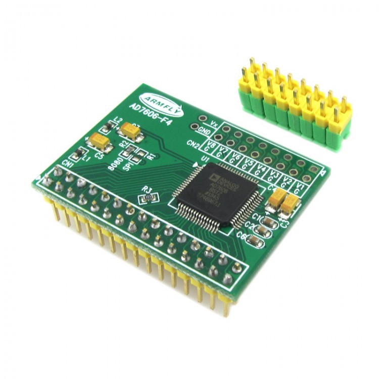
16Bits ADC 8CH Synchronization AD7606 DATA Acquisition Module 200Ksps Board
Tip : To facilitate your choice , PCB board analog input front -row pin (2x8/2.54mm pitch ) default not weld .
We will be giving away 2x8 's double needle and eight jumpers from the customer's own choice is up welding, soldering or down .
1, using high-precision 16-bit ADC chip AD7606
2,8 analog inputs. 1M ohm impedance.[No negative supply, there is no front-end analog amplifier can be connected directly to the sensor output]
3, the input range of plus or minus 5V, plus or minus 10V. By IO control.
4, Resolution 16.
5, the maximum sampling frequency sampling rate of 200ksps.
Supports eight sampling settings file (which can effectively reduce the jitter)
6, built-in benchmark
7, a single 5V power supply
8, SPI Interface, or 16-bit bus interface. Interface IO level can be 5V or 3.3V.
We AD7606 module factory default is 8080 parallel interface.
If SPI interface mode, you need to modify R1 R2 resistor configuration.
Parallel Mode Jumper: R1 floating (not stickers), R2 10K resistor paste
SPI interface mode jumper: R1 stickers 10K resistor, R2 floating (not stickers)
AD7606 configuration is very simple, it has no internal registers.
Range and over-sampling parameters are controlled via an external IO.
Pulse frequency sampling rate provided by the microcontroller or DSP control.
AD7606 must use a single 5V supply.
Level communication interface between the AD7606 and SCM controlled by VIO pin.
That VIO power supply must be connected to the microcontroller can be 3.3V can also be 5V.
[Module Pin Description]
OS2 OS1 OS2: a combination of state selection oversampling mode.
000 means no oversampling, the maximum sampling rate of 200ksps.
001 represents two times oversampling, which is the hardware inside collected two samples averaging
010 represents four times oversampling, which is the hardware inside collect four samples averaged
011 represents eight times oversampling, which is the hardware inside collected eight samples averaged
100 represents 16 times oversampling, which is the hardware inside collected 16 samples averaged
101 represents 32 times oversampling, which is an internal hardware averaging collected 32 samples
110 represents 64 times oversampling, which is the hardware inside collected 64 samples averaged
Oversampling ratio is higher, the longer the ADC conversion time, the lower the maximum sampling frequency can be obtained.
CVA, CVB: AD conversion start control signal channel 1-4 decision CVA, CVB decided 5-8 channels.
Two signals can stagger a short time, in general, can be CVA, CVB parallel together.
RAGE: Select the range of 0 means plus or minus 5V, 1 indicates negative 10V.
RD: Read signal
RST: Reset signal
Busy: Busy Signal
CS: chip-select signal
FRST: first a channel samples indicating signal
VIO: communication interface level
DB0 - DB15: Data Bus
[16 parallel mode wiring diagram --- AD7606 also supports 8-bit bus mode, see the AD7606 data sheet
MCU side AD7606 module
GND <----- ground
+5 V <----- 5V power supply
RAGE <----- can also be connected to the GPIO connected fixed level
OS2 <----- can also be connected to the GPIO connected fixed level
OS1 <----- can also be connected to the GPIO connected fixed level
OS0 <----- can also be connected to the GPIO connected fixed level
CVA <----- access the GPIO (output) is used to start AD conversion [Recommended pick pin with PWM output capability]
CVB <--- |
RD <----- 8080 bus read signal NOE
RST <----- GPIO output hardware reset AD606
Busy -----> GPIO input AD606 being converted instructions. [Recommended connection with external pin interrupt capability]
CS <----- 8080 bus chip select NCS
VIO <----- microcontroller power supply
DB0-DB15 -----> 8080 data bus (16)
FRST may take
[SPI interface mode wiring diagram
MCU side AD7606 module
GND <----- ground
+5 V <----- 5V power supply
RAGE <----- any output GPIO, can be accessed by a fixed level
OS2 <----- any output GPIO, can be accessed by a fixed level
OS1 <----- any output GPIO, can be accessed by a fixed level
OS0 <----- any output GPIO, can be accessed by a fixed level
CVA <----- access the GPIO (output) is used to start AD conversion [Recommended pick pin with PWM output capability]
CVB <--- |
RD / SCLK <----- SPI bus clock SCK
RST <----- any output GPIO, for hardware reset AD606
Busy -----> GPIO input, AD606 being converted instructions. [Recommended connection with external pin interrupt capability]
CS <----- SPI bus chip select SCS
VIO <----- microcontroller power supply
DB7 (DOUTA) -----> SPI bus data lines MISO
DB14 - DB15 may pick
FRST may take
Software implementations [1] --- timing acquisition of SPI example we offer document using this program, see bsp_spi_ad7606.c
In the timer interrupt service routine implementation:
Timer interrupt ISR:
{
Interrupt entry;
8 reads the sampling results are stored in the RAM channel; ----> read is the last record collection for continuous acquisition, it is not related to the
Start next ADC acquisition; (flip CVA and CVB)
Interrupt return;
}
Timer frequency is the ADC sampling frequency. This mode can not connect busy port cable.
Software implementations [2] --- timed 8080 acquisition of the interface we provide an example of using this program, see bsp_ad7606.c file
Configure CVA CVB pin PWM output mode, the sampling period is set to the desired frequency; ---> After the MCU will produce a very stable AD conversion cycle signal
The busy port line is set to interrupt falling edge trigger mode;
External interrupt ISR
{
Interrupt entry;
8 reads the sampling results of the channel stored in the RAM;
Interrupt return;
}
[1 and 2, the differences in implementations of software-timed acquisition]
(1) Option 1 may be less busy lines, but the other main interrupt service routine or temporary closure of the global interrupt when ADC conversion cycle may cause a slight jitter.
(2) Option 2 can ensure the stability of the acquisition of the clock, because it is generated by the MCU hardware, but need more then a BUSY mouth lines.
Package included:
- 1 PCS x 16Bits ADC 8CH Synchronization AD7606 DATA Acquisition Module 200Ksps