| Quantity | 3+ units | 10+ units | 30+ units | 50+ units | More |
|---|---|---|---|---|---|
| Price /Unit | $39.05 | $38.26 | $37.06 | $35.47 | Contact US |
 AD2S1210 N1 16Bit R/DC High Performance Resolver Transformer Demodulation Module 15.8Vpp Excitation Amplitude
$77.75
AD2S1210 N1 16Bit R/DC High Performance Resolver Transformer Demodulation Module 15.8Vpp Excitation Amplitude
$77.75
 GC-1201S Two-master One-slave Isolated RS485 Hub Repeater Double Electrical Isolation with 12V Power Supply
$36.58
GC-1201S Two-master One-slave Isolated RS485 Hub Repeater Double Electrical Isolation with 12V Power Supply
$36.58
 GC-1201S Two-master One-slave Isolated RS485 Hub Repeater Double Electrical Isolation Support for Modbus Protocol
$33.75
GC-1201S Two-master One-slave Isolated RS485 Hub Repeater Double Electrical Isolation Support for Modbus Protocol
$33.75
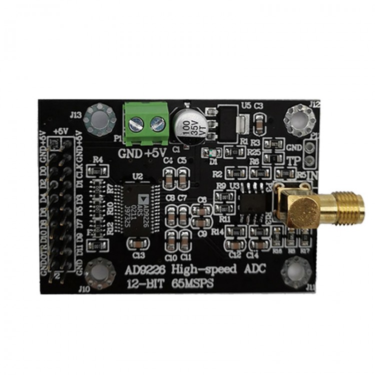
AD9226 SSOP28 Version High-Speed ADC Module 65M Sampling Data Acquisition For FPGA Development Board
Advantages:
- High-speed signal acquisition, analog-to-digital conversion module
- Power supply voltage: DC-5V
- Module communication protocol: 13-bit parallel SPI
- Module provides routine: For Verilog FPGA source code
- Routine platform: For QuartusII EP4CE15F17C8
Attention:
- Module's interfaces are clear and the performance is stable. Please use the schematic diagram provided by our shop for functional verification under the corresponding experimental conditions.
- The basic parameters of this module are provided below, and the module information PDF file and the source code of routine are provided. Project files are not provided. Buyers can consult customer service if they have operational problems.
- Before using the module, read the details of this module, understand the power supply and usage restrictions to avoid damage to the module due to improper operation.
- All the modules have been tested before delivery.
- Provide module schematic diagram in PDF, FPGA test reference program, module instruction and chip manual.
Module Parameters:
* Module model: AD9226_01
* Module type: analog to digital conversion module
* Sampling rate: 65M SPS (Max.)
* ADC resolution bits: 12 bits
* Input voltage range: 10VPP (±5V) (signal impedance: 50Ω)
* Power supply: 5V DC (Min: 4.75V. Typ: 5V. Max: 5.25V)
* Provide example: For Verilog FPGA source code
* Example platform: For QuartusII EP4CE15F17C8
* Communication protocol: 13-bit parallel SPI
* Communication signal level: 3.3V
* Input impedance: 50 ohm
* Number of input channels: 1 channel
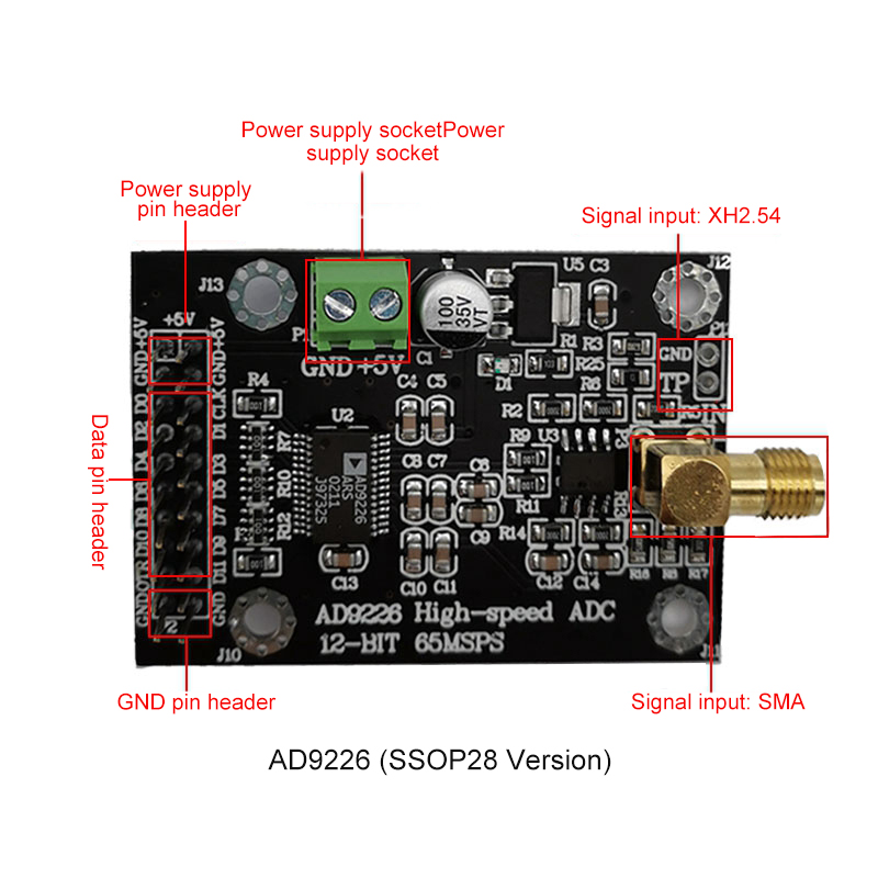
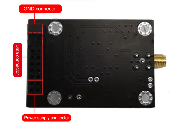
* Input interface: SMA tuner/XH2.54 hole
* Reference voltage: internal 2V
* -3dB analog bandwidth: 320MHz
* Output mode: parallel data
* Module features: high-speed ADC acquisition
* Module application: high-speed signal acquisition
* Module weight: 16g
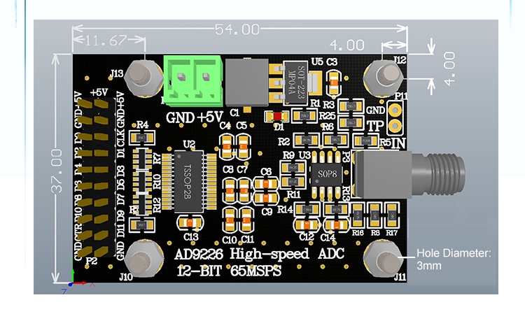
* PCB Size: 54*37*23mm (LxWxH)
* Module interface type: 13-bit data SPI parallel
Module Description:
The high-speed AD of this module uses 12-bit high-speed A/D converter AD9226. AD9226 uses a multi-stage differential pipeline architecture, with a maximum sampling rate of 65MSPS. The chip is powered by a single power supply, with a sample holder and reference voltage source on-chip, which simplifies the design of peripheral circuits. Meet industrial-grade applications, and ensure no missing codes in the entire operating temperature range.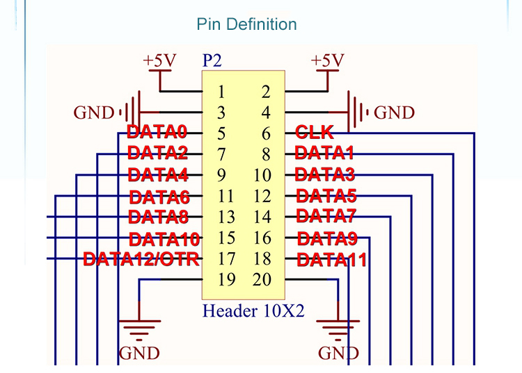
Package Included:
- 1 x Set of ADC Module
Precautions:
(1) Power supply should not be over-voltage.
(2) Do not use longer cables for data communication.
(3) It is recommended to use SMA shielded wire input for high-speed signals.
(4) Direct code: (-5V~+5V, 12-bit value increment), complement code: (D11 is the sign bit, D10~D0 is a number).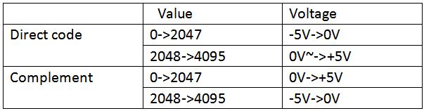
Module Test Pictures:
1M Square Wave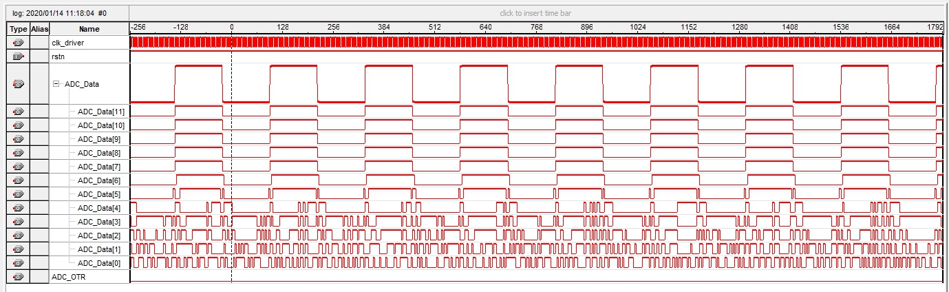
1M Triangle Wave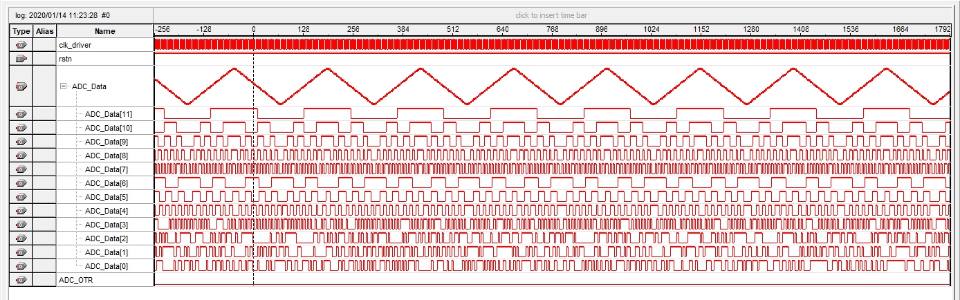
1M Sine Wave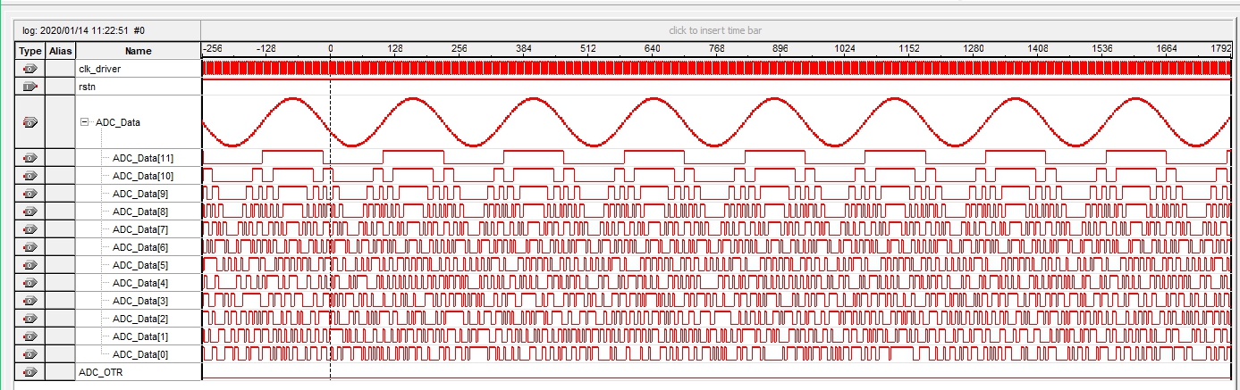
6M Sine Wave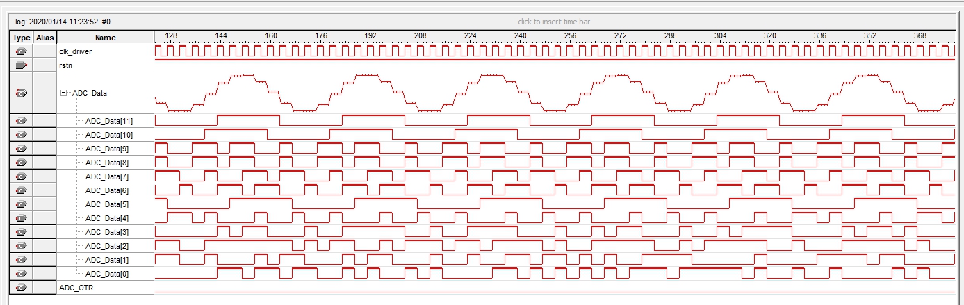
200K Sine Wave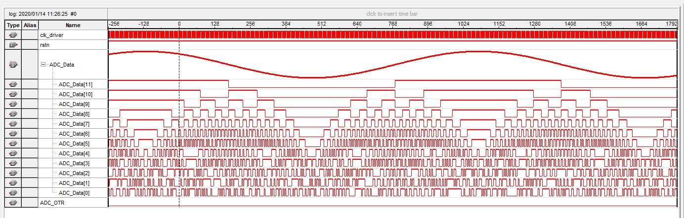
FAQ:
Q1: The input voltage has not reached 5V, and the output data has reached the maximum value.
A1: Check whether the power supply is +5V. The module power supply is too low, it will affect the measurable voltage range.
Q2: A certain voltage has been input, but the measured data can only correspond to half of the input voltage or lower.
A2: Please confirm that the input signal is 50 ohm impedance. (The input impedance of the module is 50 ohms. If the input signal drive capacity is insufficient, the voltage will drop by half or more after input to the board. Use a multimeter or oscilloscope to measure the actual voltage at the input of the module, and the voltage measured by the module is the same as that value).
Q3: The voltage has been input to -5V, but the data cannot reach the minimum value of 0 (may be 2, 5 or other), or when 5V is input, the data is only close to the maximum value.
A3: Affected by the tolerances of the on-board components, there may be slight differences in the input voltage after being conditioned by the signal preprocessing circuit, or the accuracy of the signal itself will also be affected to a certain extent (display input -5V, actually only input -4.99V), this In this case, if the input is slightly less than -5V, the data can reach the minimum value of 0.
Q4: What is the purpose of OTR pin? Is it data?
A4: OTR is the data overflow flag. For example, this module is designed with an input range of plus or minus 5V, and if the input exceeds +5V or exceeds -5V, this pin will be set high.
Chip Introduction:
AD9226 is powered by a single power supply. It features 12-bit precision, 65Msps high-speed analog-to-digital converter, on-chip integrated high-performance sample-and-hold amplifier (Sample-and-hold amplifier SHA) and reference voltage source. AD9226 uses a multi-stage differential pipeline structure with error correction logic to ensure accurate 12-bit data at 65Msps sampling rate. At the same time, AD9226 also has lower power consumption (475mw) and higher SNR (69dB).
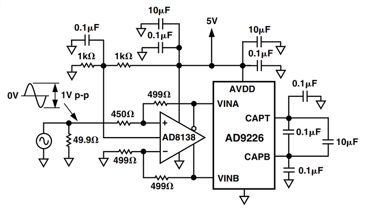
Chip Typical Application Diagram: