| Quantity | 3+ units | 10+ units | 30+ units | 50+ units | More |
|---|---|---|---|---|---|
| Price /Unit | $3,647.19 | $3,572.76 | $3,461.11 | $3,312.24 | Contact US |
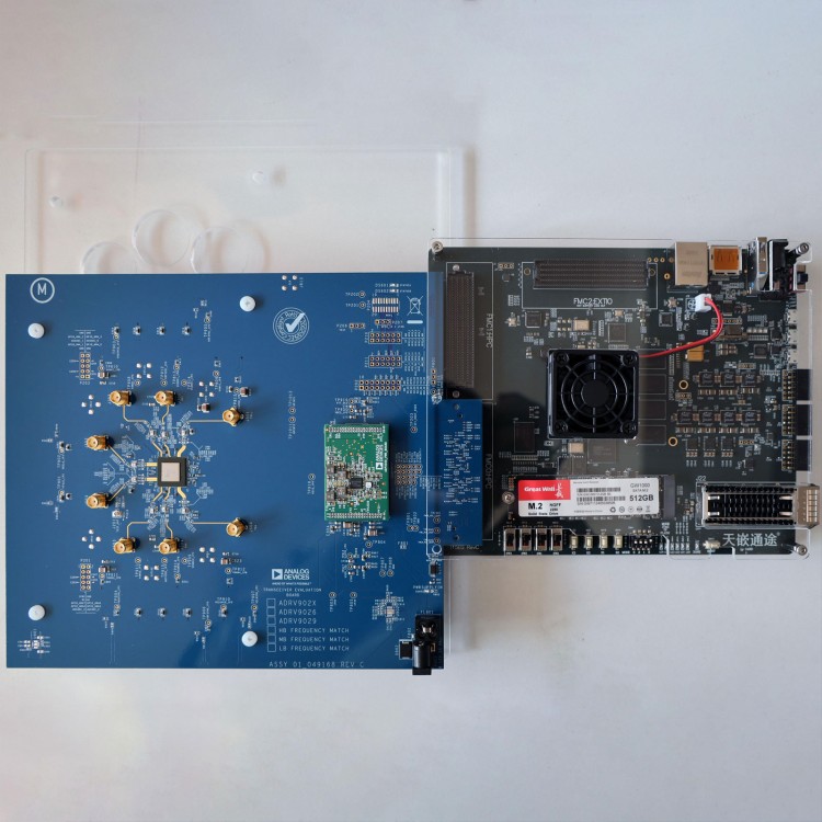
ADRV9026 RF Sub Board 4-Channel 650MHz-6000MHz Wideband RF Transceiver Board with MPSOC Development Board Kit
Description:
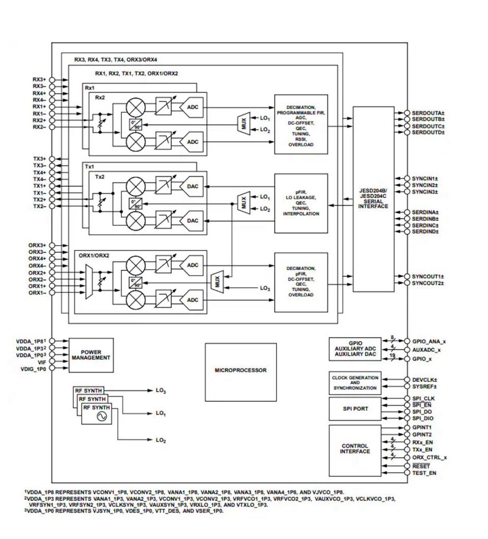
- ADRV9026 is a highly integrated RF agile transceiver that offers four independently controlled transmitters, dedicated observation receiver inputs for monitoring each transmitter channel, four independently controlled receivers, an integrated frequency synthesizer, and digital signal processing capabilities, forming a complete transceiver solution. This device provides the performance required for various cellular infrastructure applications, such as small cellular base station radios, 3G/4G/5G macro systems, and large-scale multiple input/multiple output (MIMO) base stations.
Key Features:
- 4 differential transmitters
- 4 differential receivers
- 2 observation receivers, each with 2 inputs
- Center frequency: 650MHz to 6000MHz
- Maximum receiver bandwidth: 200MHz
- Maximum transmitter bandwidth: 200MHz
- Maximum transmitter synthesis bandwidth: 450MHz
- Maximum observed receiver bandwidth: 450MHz
- Fully integrated independent decimal N-division RF synthesizer
- Fully integrated clock frequency synthesizer
- Multi chip phase synchronization for all local oscillators and baseband clocks
- Support for TDD and FDD applications
- 16Gbps JESD204B/JESD204C digital interface
Characteristics:
- Dual channel design: supports two independent receiving and sending channels, suitable for various application scenarios.
- Frequency range: the working frequency covers 300MHz to 6GHz, adapting to different wireless communication standards.
- Broadband width: supports signal bandwidth up to 100MHz, suitable for broadband communication needs.
- High performance ADC/DAC: integrating high-resolution analog-to-digital converters (ADCs) and digital-to-analog converters (DACs) to provide excellent dynamic range and low noise performance.
- Digital signal processing (DSP): built-in DSP function, capable of implementing complex signal processing algorithms such as spectrum sensing and signal demodulation.
- Low power design: optimized power performance, suitable for battery powered application scenarios.
- Programmable gain amplifier (PGA): adjustable gain to adapt to different signal strengths and enhance reception flexibility.
Applications:
- Wireless base station: used for signal transmission and reception of 4G/5G base stations.
- Satellite communication: supports the reception and transmission of satellite signals.
- Internet of Things (IoT): suitable for low-power wide area network (LPWAN) applications.
- Military communication: a highly reliable wireless communication solution.
Interface and Configuration:
- SPI interface: used for communication with micro-controllers or FPGAs.
- GPIO pin: a configurable general-purpose input/output pin that facilitates external interface control.
- Clock synchronization: supports external clock input to ensure the stability of the system clock.
Performance:
- Receiving sensitivity: superior receiving sensitivity, suitable for weak signal environments.
- Linearity: excellent linearity ensures the authenticity of the signal.
- Phase noise: low phase noise performance enhances signal clarity.
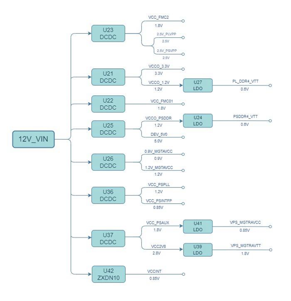
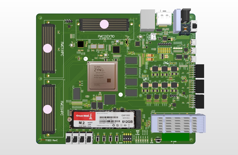
MPSOC:
Startup Mode:
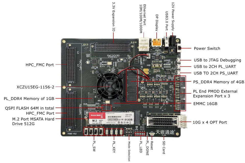
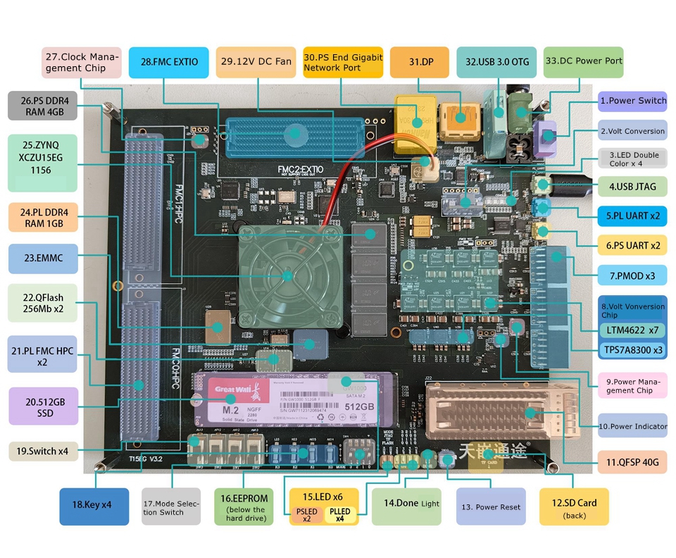
- The onboard USB to JTAG module can achieve JTAG boot.
- Dual-channel Quad-SPI flash memory (programmed online via JTAG).
- Start from TF/SD card (programmed through card reader)
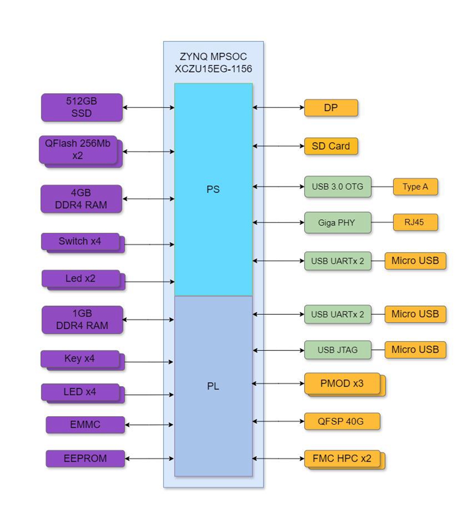
Memory Storage:
- PS external 4GB DDR4 64-bit
- PL plug-in 1200MHz/2400Mbps DDR PL 512MB DDR4 component memory (256Mbx16 device), which is 1GB wide 16 bit.
- 8KB IIC EEPROM.
- Dual 64MB Quad-SPI flash can be used for booting
- TF/SD card slot
- M.2 SATA 512G memory
Control and I/O:
- 4 PL buttons KEY
- 4 PL dip switches SWITCH
- 6 PL LEDs
- Start mode dip switch
- Global reset button
Expansion Connector:
- 2 FMC-HPC (compatible with FMC-LPC) connectors (16 GTH transceivers, 64 differential user-defined signals)
- 1 FMC-LPC connector
- 2-channel PMODPL external expansion port
- 1-channel PMODPS external expansion port
Communication Network:
- 10/100/1000Mb/s RGMII communication. Serial GMII interface supports 1GB/s SGMII interface
QSFP has four optical ports, which can be divided into four separate optical ports. Speed>10G
- Two PS UART to USB Bridge
- Two PL UART to USB Bridge
- RJ45 Ethernet connector
- DP display interface
- The USB HOST interface can connect to USB flash drives, keyboards, and mice.
Clock Schemes:
- CDCM6208 programmable clock, supplying the following clocks:
> 33.333M is used as the input clock for PS.
> 26M serves as the clock for USB 3.0 interface.
> 27M serves as the clock for the DP port.
> 125M serves as the clock for SATA.
> 74.25M and 100M as user PL clocks
- Additionally, there are two specialized differential crystal oscillators:
> 156.25M provided to GTH clock can be used for 10G optical port communication
> 200M is provided to PL as a reference clock for PLDDR4 or as a clock for other PLs
Package Included:
- 1 x RF Sub Board
- 1 x MPSOC Development Board Kit