| Quantity | 3+ units | 10+ units | 30+ units | 50+ units | More |
|---|---|---|---|---|---|
| Price /Unit | $315.98 | $309.53 | $299.86 | $286.96 | Contact US |
 Red Frame Music Tesla Coil 10 Mini 0-100W High Power Musical Coil Touchable Lightning Support Bluetooth Control
$39.37
Red Frame Music Tesla Coil 10 Mini 0-100W High Power Musical Coil Touchable Lightning Support Bluetooth Control
$39.37
 Black Frame Music Tesla Coil 10 Mini 0-100W High Power Musical Coil Touchable Lightning Support Bluetooth Control
$50.95
Black Frame Music Tesla Coil 10 Mini 0-100W High Power Musical Coil Touchable Lightning Support Bluetooth Control
$50.95
 Magnetic Levitation DIY Magnetic Levitation Module Assembled with Acrylic Shell 150G Load Limit
$39.68
Magnetic Levitation DIY Magnetic Levitation Module Assembled with Acrylic Shell 150G Load Limit
$39.68
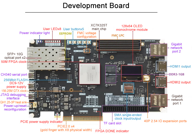
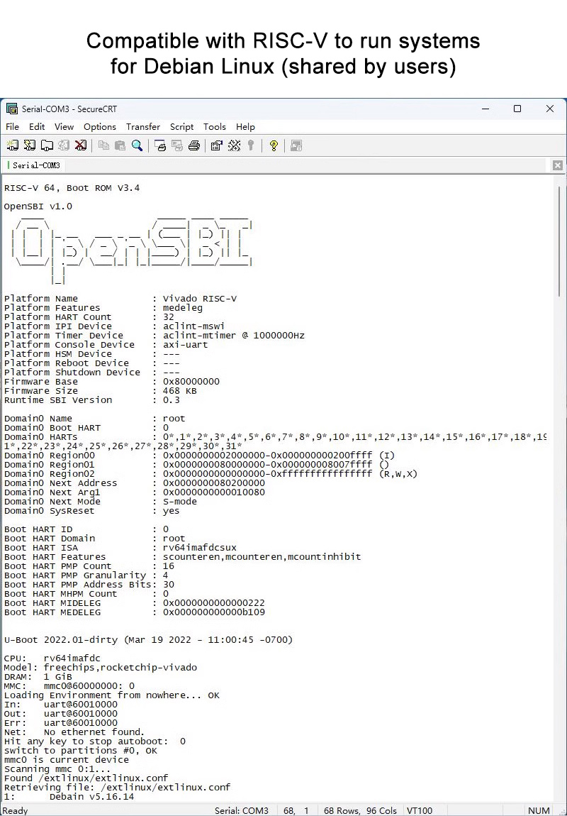
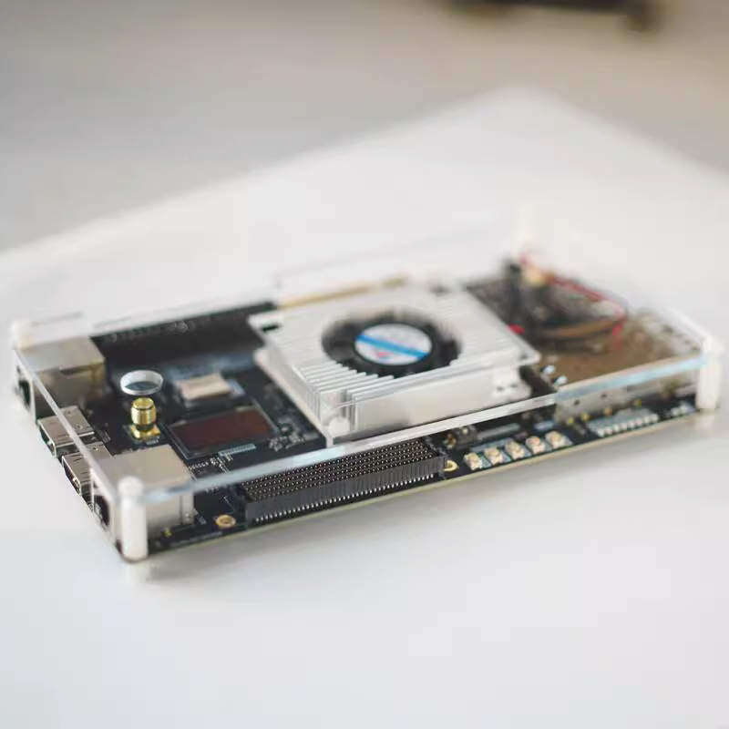
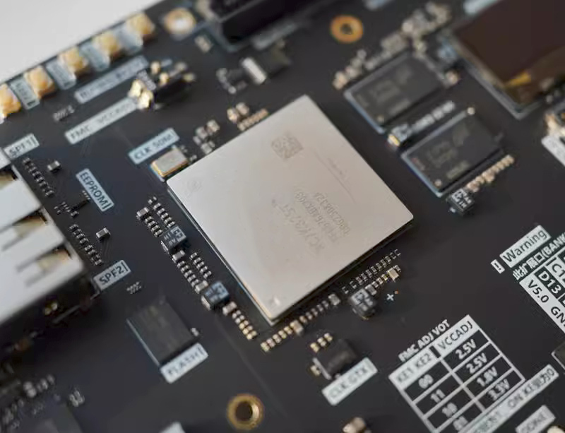
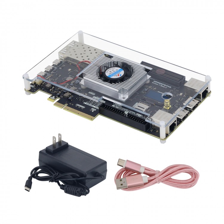
K7 Base C XC7K325T Development Board FPGA Development Board with Dual Gigabit Port for Kintex DIY
Features:
- FPGA development board
- There are many on-board interfaces
- Abundant on-chip resources
- MCU-grade chip makes it cost-effective
- Development software companion version VIVADO2020.1
Chip resource:
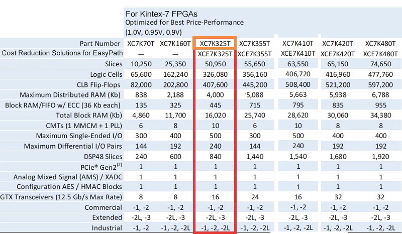
- Main chip model: XC7K325T-2FFG676I
- Chip grade: Industrial grade
- Recommended maximum clock speed: PLL/MMCM recommends a maximum speed of 709M
- DDR specifications: MT41K256M16TW-107, 32-bit, 1GByte, 1600M
- Logic cells (LC): 326,080
- Slices: 50,950
- DSP unit multiplier: 840
- Trigger: 407,600
- RAM: 160, 20Kbit
- Device temperature range: -40 to 85°C
- Speed class: -2
- Number of GTX: 16
Parameter description of the functional interface of the development board:
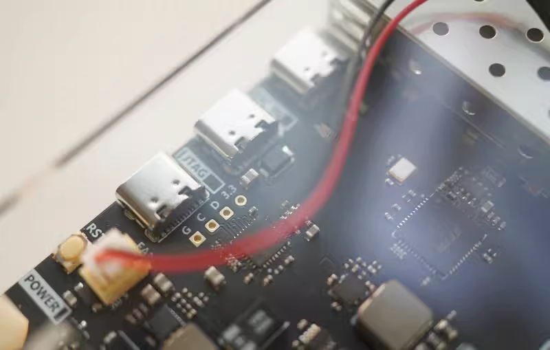
- Power supply mode: 9-12V/3A customized power supply with TYPE-C interface, power supply through DC-IN
- Heat sink connector: Heat sink connector with a GH1.25-3P connector on board
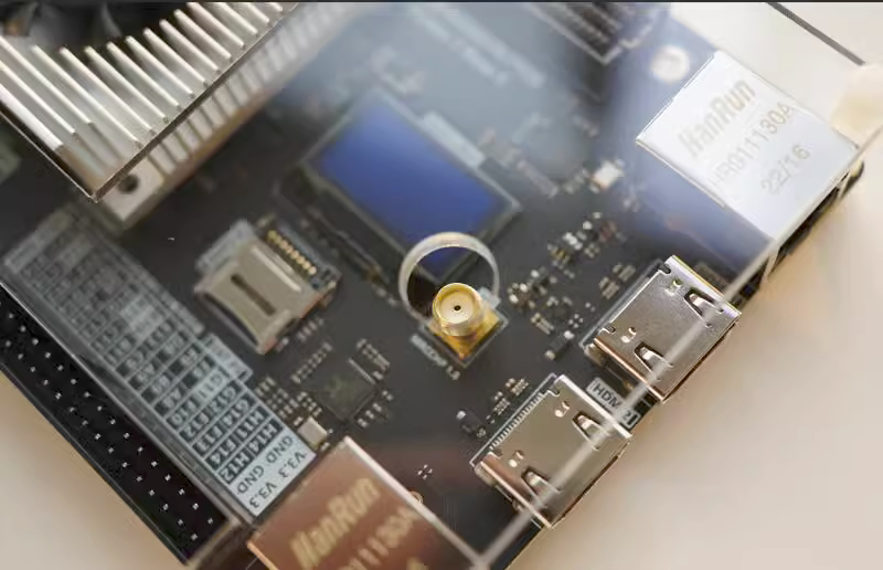
- Clock resources: 50M single-ended crystal oscillator, 156.25M differential crystal oscillator, and one SMA clock interface
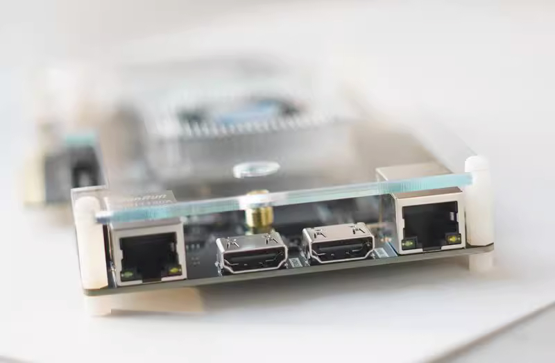
- Ethernet: Two Gigabit RGMII ports. The models of the ports are RTL8211E-VL and RTL8211E-VB
- User buttons: 5 user buttons, 1 power-on/reset button, support chip reset and reconfiguration
- Debugger: On-board TYPE-C interface downloader debugger. Support online debugging and downloading
- Serial port: CH340 serial port with one TYPE-C interface
- SD card slot: One flip-top TF card holder, support SPI interface
- HDMI interface: two channels support output up to 1080 at 60HZ
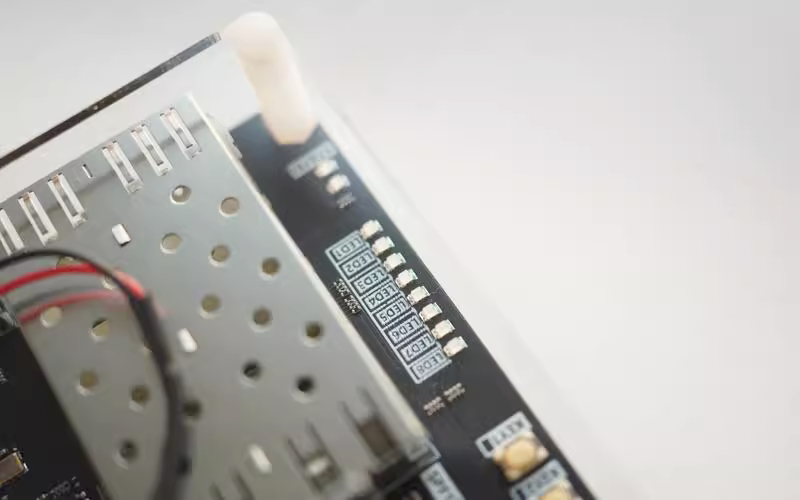
- On-board LEDs: 2 power status LEDs, 8 FPGA LEDs, DONE, PCIE power supply
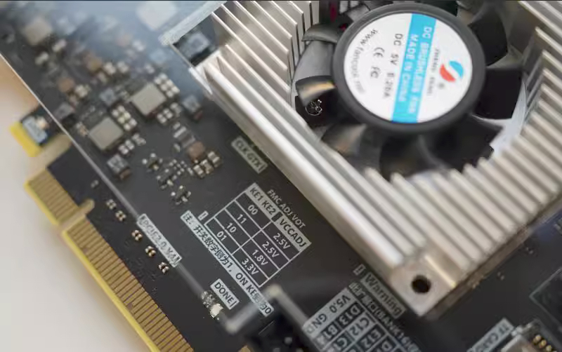
- Set Switch: A voltage DIP switch that sets the LA differential pin of the FMC interface
- Onboard FLASH: MX25L25645G particles, 32MByte space
- EEPROM: A 24C02 EEPROM memory chip
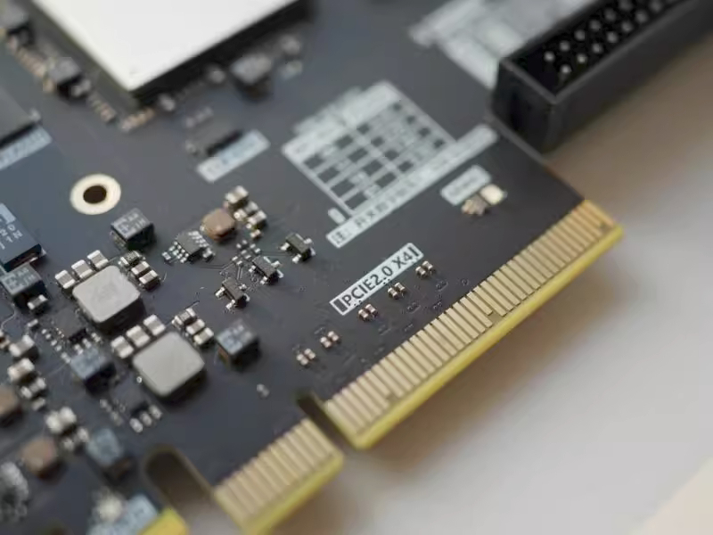
- PCIE interface: PCIE 2.0 X8, need X8 or X16 physical slot
- On-board OLED module: 0.96-inch SSD1306-driven OLED module, 128x64 monochrome
- IO expansion port: FMC LPC and 40P standard 2.54 double-row expansion port; FMC includes LA (34 pairs differential + 2 pairs of clock differential) and 1 pair of GTX; The 40PIN 2.54 IO expansion ports contains only 34pcs 3.3V single-ended IO
- Optical communication interface: 2CH SFP+, support 10G optical communication
Attention:
- FMC uses ANK12 and 13 for HR BANK, and LVDS only supports 2.5V LVDS_25.
- The 40P 2.54 expansion ports use BANK16 for HR BANK, and the voltage is fixed 3.3V single-ended.
Package Included:
- 1 x Development board
Note:
- SD card is not included.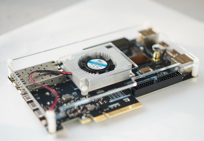


 for Raspberry Pi")


 for Raspberry Pi")