| Quantity | 3+ units | 10+ units | 30+ units | 50+ units | More |
|---|---|---|---|---|---|
| Price /Unit | $13.61 | $13.33 | $12.92 | $12.36 | Contact US |
 LC29HBS Dual Band Multi-constellation Base Station GNSS Module + Antenna with RTK Function GPS/BDS/Galileo/QZSS/GLONASS
$45.10
LC29HBS Dual Band Multi-constellation Base Station GNSS Module + Antenna with RTK Function GPS/BDS/Galileo/QZSS/GLONASS
$45.10
 LC29HBS Dual Band Multi-constellation Base Station GNSS Module with RTK Function GPS/BDS/Galileo/QZSS/GLONASS
$33.44
LC29HBS Dual Band Multi-constellation Base Station GNSS Module with RTK Function GPS/BDS/Galileo/QZSS/GLONASS
$33.44
 LC29HDA Dual Band Multi-constellation Mobile Station GNSS Module + Antenna with RTK Function GPS/BDS/Galileo/QZSS/GLONASS
$49.96
LC29HDA Dual Band Multi-constellation Mobile Station GNSS Module + Antenna with RTK Function GPS/BDS/Galileo/QZSS/GLONASS
$49.96
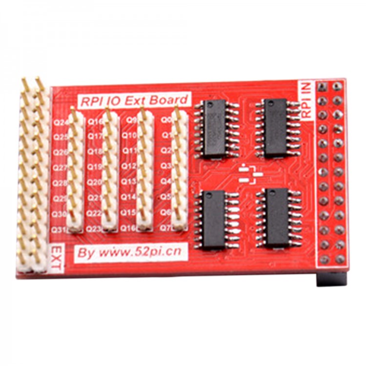
Raspberry Pi SPI GPIO IO Extended Board Raspberry Pi Infinite Cascade Connection Adapter Plate
Product Overview:
This module is designed specifically for the Raspberry Pi IO expansion Modules,which can effectively solve the Raspberry send IO port insufficient.Module uses four 74HC595 chips to expand 32 IO ports.As shown above, the top of the module will expand the IO of Raspberry Pi again that can be cascaded for more IO expansion modules can theoretically unlimited expansion.
Features:
- Expanded 32 GPIO
- Infinity connection for the same module
- Use wiring PI API,sample code
Port:
- Raspberry Pi 2*13port
- Raspberry Pi 2*13 cascade port
- Q0-Q31 expanded IO port
Product Parameters:
- Working voltage:2.4v-5v
- IO voltage:3.3v
- Expanded 32 unidirectional IO
- Connection through SPI
- 100 MHz (typical) shift out frequency
- 8-bit serial input
- 8-bit serial or parallel output
- Specified from -40C to +85C and from -40C to +125C
Typical Application:
- Drive the lattice screen
- Driver numeric display
- Drive matrix LED
How to Use
Insert the module that the silk screen says 'RPI IN'. Pay attention don’t make the direction reversed! The correct direction of insert module is above the Raspberry Pi’s PCB; The 8*4header in the module are Q0-Q31 expanded GPIO, they can connect to the peripheral through the Dupont Line. The header which near silk screen write 'EXT' expand GPIO of Raspberry Pi, user can cascade the other module or the same module.
More information
- The 74HC595,74HCT595 are high-speed Si-gate CMOS devices and are pin compatible with Low-power Schottky TTL (LSTTL). They are specified in compliance with JEDEC standard No. 7A.
- The 74HC595,74HCT595 are 8-stage serial shift registers with a storage register and 3-state outputs. The registers have separate clocks.
- Data is shifted on the positive-going transitions of the shift register clock input (SHCP).
- The data in each register is transferred to the storage register on a positive-going transition of the storage register clock input (STCP). If both clocks are connected together, the shift register will always be one clock pulse ahead of the storage register.
- The shift register has a serial input (DS) and a serial standard output (Q7S) for cascading. It is also provided with asynchronous reset (active LOW) for all 8 shift register stages. The storage register has 8 parallel 3-state bus driver outputs. Data in the storage register appears at the output whenever the output enable input (OE) is LOW.
Function table
- Control Input Output Function
- SHCP STCP OE MR DS Q7S Qn
- X X L L X L NC a LOW-level on MRonly affects the shift registers
- X ↑ L L X L L empty shift register loaded into storage register
- X X H L X L Z shift register clear; parallel outputs in high-impedance OFF-state
- ↑ X L H H Q6S NC logic HIGH-level shifted into shift register stage 0. Contents of all
- shift register stages shifted through, e.g. previous state of stage 6
- (internal Q6S) appears on the serial output (Q7S).
- X ↑ L H X NC QnS contents of shift register stages (internal QnS) are transferred to
the storage register andparallel output stages
- ↑ ↑ L H X Q6S QnS contents of shift register shifted through; previous contents of the
- shift register is transferred to the storage register and the parallel
- output stages
- H = HIGH voltage state;
- L = LOW voltage state;
- ↑= LOW-to-HIGH transition;
- X = don’t care;
NC = no change;
Z = high-impedance OFF-state.
Package included:
- 1 x Extended Board