| Quantity | 3+ units | 10+ units | 30+ units | 50+ units | More |
|---|---|---|---|---|---|
| Price /Unit | $430.20 | $421.42 | $408.25 | $390.69 | Contact US |
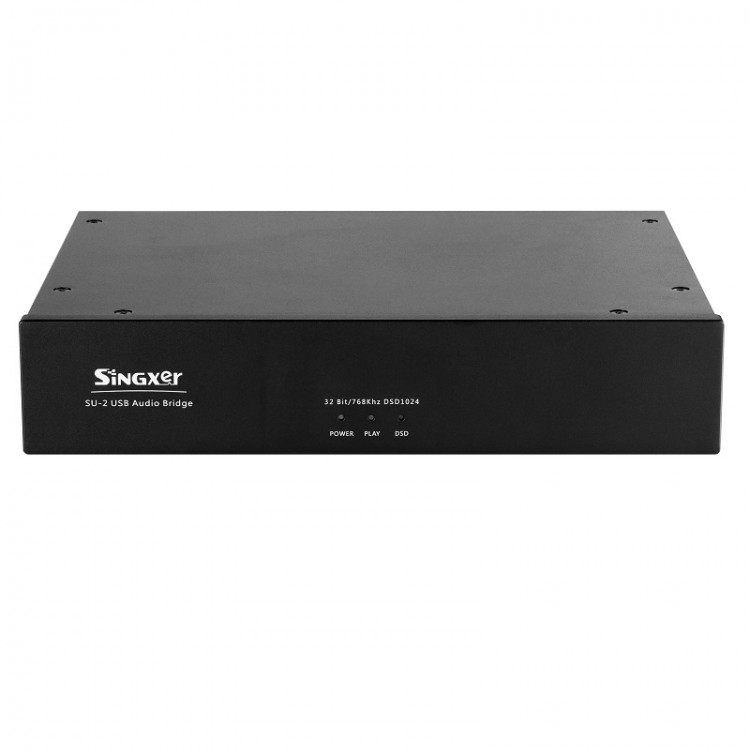
Singxer SU-2 DSD1024 USB Digital Interface Femtosecond Clock Ship Interface Audio Interface (220V)
Product Description:
The SU-2 digital interface is a high-performance USB digital audio interface. It adopts a microprocessor with the latest ARM Cortex-M4 as the core to control the USB data. SU-2 adopts the self-developed ultra-low jitter clock system (ACCUSILICON's AS-318B series, which achieves ultra-low jitter at the femtosecond level). It uses large-capacity FPGA as the core of digital audio data processing, and has a standard USB2.0 input interface , rich output interface, including XLR balanced output AES, coaxial RCA and BNC, I2S interface with HDMI socket output, perfect master clock and word clock (WCLK) output. SU-2 supports external 10Mhz clock input, using common 50 ohm input impedance design.
The SU-2 is not just a USB interface, it can also be used as an independent master clock product.
1. When used as an independent master clock, it can output a word clock of 44.1K-384K or a master clock of 22.5792Mhz-49.152Mhz. (When not connected to USB, it will be used as the master clock device by default)
2. When using external 10Mhz clock input, it can also be used as a frequency converter; it supports 10Mhz to 44.1K-384K word clock, or output 22.5792Mhz-49.152Mhz master clock.
SU-2 is a brand-new USB interface developed by us to replace the original SU-1; PCM sampling rate supports up to PCM 768K, and DSD supports up to DSD1024. Using large-scale FPGA as the core of arithmetic processing, we decentralized some of the FPGA algorithm technology of the flagship interface SU-6 to the SU-2; its positioning in the mid-to-high-end interface mainly uses the following three unique technologies:
1. Full isolation technology (ground wire isolation), using 150Mbps full isolation chip, can completely isolate the interference from the PC;
2. Source synchronization technology and FPGA shaping technology to reshape the isolated I2S signal; thereby eliminating the additive jitter caused by the isolation chip;
3. Self-developed clock system, adopt ACCUSILICON's high-performance crystal oscillator, low phase noise, and low jitter; you can also choose an external 10Mhz clock to support various atomic clocks, constant temperature crystal oscillators, and GPDSO input.
Technical Index:
Sampling rates supported by each output interface:
PCM: 44.1KHz, 48KHz, 88.2KHz, 96KHz,
176.4KHz, 192KHz, 352.8KHz, 384KHz, 705.6KHz, 768KHz
[Among them, I2S out supports all sampling rates, S/PDIF supports up to 384KHz, DOP128]
2. 8 MHz (DSD64)-DOP, native
5.6 MHz (DSD128)-DOP, native
11.2 MHz (DSD256)-DOP, native
22.5792 MHz (DSD512)-DOP, native
45.1584 MHz (DSD1024)-native
[Among them, I2S out supports all DSD formats, S/PDIF and AES/EBU support DSD128 DOP mode]
Bit width: up to 32 bit over I2S output
Up to 24 bit over S/PDIF
Electrical Standards of Each Interface:
1. The USB input socket is a standard USB-B type female socket, and the USB power supply range is 4.5V-5.1V;
2. The RCA interface outputs a standard S/PDIF signal with a level of 550mV (connected to a standard load) and an output impedance of 75 ohms;
3. The power input is AC, and an imported transformer is used for power supply.
Details:
1. We attach great importance to the design of power supply circuits, using LDOs with high performance, low noise and fast response as the main power supply. The entire board uses multiple independent LDO power supplies, and the clock part even uses ADI's ultra-low noise LDO, which lays a solid foundation for ensuring the ultimate output performance.
2. The PCB motherboard adopts a 4-layer circuit board design to ensure a complete ground plane and power layer. A high-speed digital design method is used to ensure the signal integrity and power integrity of the entire board. The clock signal is specially processed, and the grounded design and precise impedance control are adopted to ensure the clock signal quality and improve its anti-interference ability. The input and output signals follow the standard design, especially the USB high-speed signals use 90 ohm differential impedance control.
System Compatibility:
1. Windows 7, Windows 8, Windows 10; 32/64 bit, need to install special driver
2.Native MacOS 10.6 and later, using the system's own driver
3. Native Linux with UAC2 compliant kernel, using the system's own driver, (tested on Ubuntu and Daphile systems, based on Intel X86 platform)
4. Android OS 4.2 and above, the device needs to support OTG function, generally speaking, the system above Android 9.0 is supported by default. It is recommended to use with a special player below 9.0.
I2S Interface Uses HDMI Socket Output:
1. 3.3V LVDS differential signal;
2. DSD ON signal, 5V power supply (small current),CPLD has been processed inside the MUTE signal, and there is no need to output the MUTE signal;\
3. The DSD ON signal can be defined by itself. The DSD ON signal can be arbitrarily output to the PIN13, 14, 15, 16 pins of the socket.
Flexible I2S and Clock Output Configuration:
1. Switches 1-4 correspond to the PIN13-16 pins of the HDMI socket. Pull to the ON position, it means that the HDMI PIN has the function of DSD_ON.
2. Switches 5 and 6 are the modes that configure the clock output:
When the switch 5 is OFF, the clock outputs MCLK, and when it is ON, the clock outputs WCK.
Switch 6 configures the frequency of MCLK, which is 22.5792M / 24.576M when OFF, and 4.5.1584M / 49.152M when ON;
3. Switch 7 can set the left and right channels in DSD mode in I2S signal separately.
4. Switch 8 can set the BCLK line sequence in the I2S signal; when OFF, PIN4 is BCLK + and PIN6 is BCLK-;
5. Switch 9 can set the line sequence of LRCLK in I2S signal; when OFF, PIN7 is LRCLK + and PIN9 is LRCLK-;
6. Switch 10 can set the line sequence of DATA in I2S signal; when OFF, PIN1 is DATA + and PIN3 is DATA-.
Case Size and Packaging:
Case L*W*H: 234mm * 170mm * 46mm, excluding the height of the feet and the protruding part of the connector on the back of the case
Stand-alone weight: 1.8kg
L*W*H of carton package: 350mm * 230mm * 110mm
Shipping package weight: 2.3kg
Package List:
-1 x Digital Interface
-1 x USB Cable
-1 x Power Cable
")
")
")
")


")
")


