| Quantity | 3+ units | 10+ units | 30+ units | 50+ units | More |
|---|---|---|---|---|---|
| Price /Unit | $42.18 | $41.32 | $40.03 | $38.31 | Contact US |
 SUP-C703S Signal Generator & Process Calibrator – mA, V, Ω, RTD, Thermocouple Output & Measurement
$156.44
SUP-C703S Signal Generator & Process Calibrator – mA, V, Ω, RTD, Thermocouple Output & Measurement
$156.44
 6000A 20µH Air Core Inductor for Dual Pulse Testing and High-Performance Electrical Experiments
$86.76
6000A 20µH Air Core Inductor for Dual Pulse Testing and High-Performance Electrical Experiments
$86.76
 DP8000 Max IGBT Pulse Generator with Internally Integrated IGBT Driver (Air Core Inductor Included)
$384.16
DP8000 Max IGBT Pulse Generator with Internally Integrated IGBT Driver (Air Core Inductor Included)
$384.16
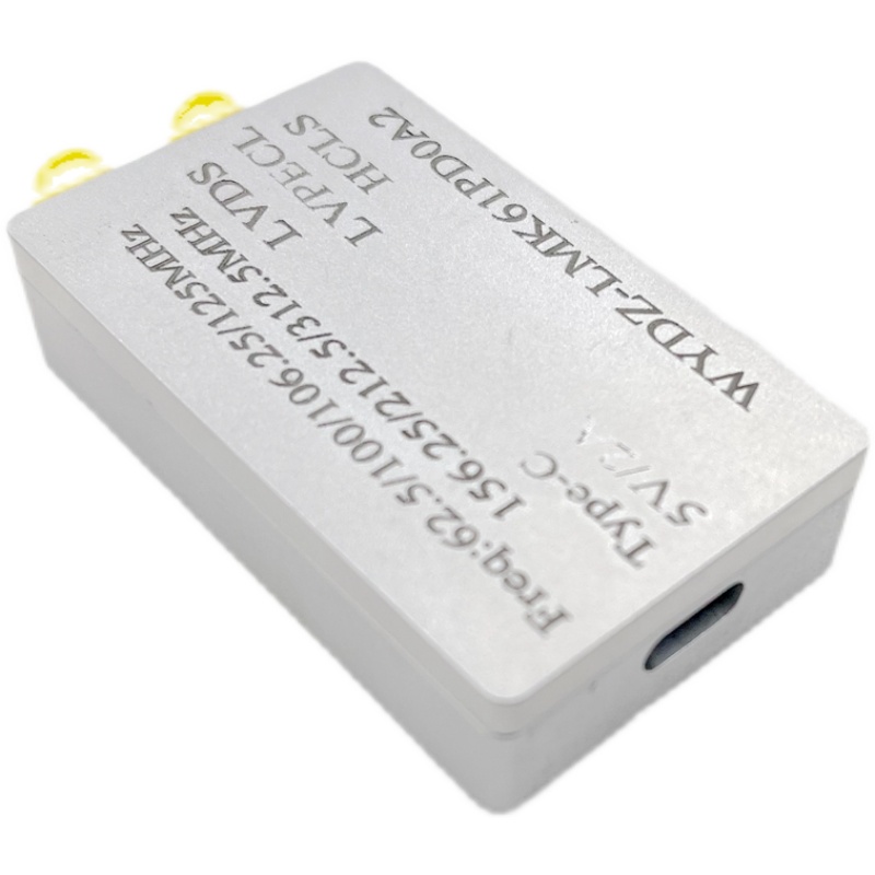
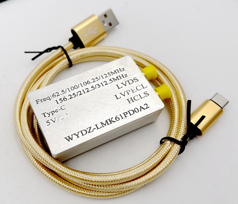
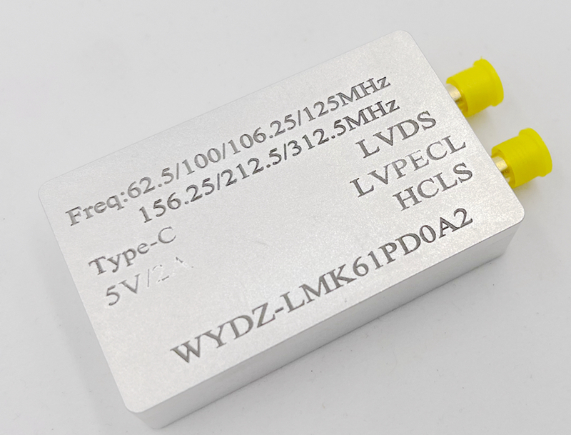
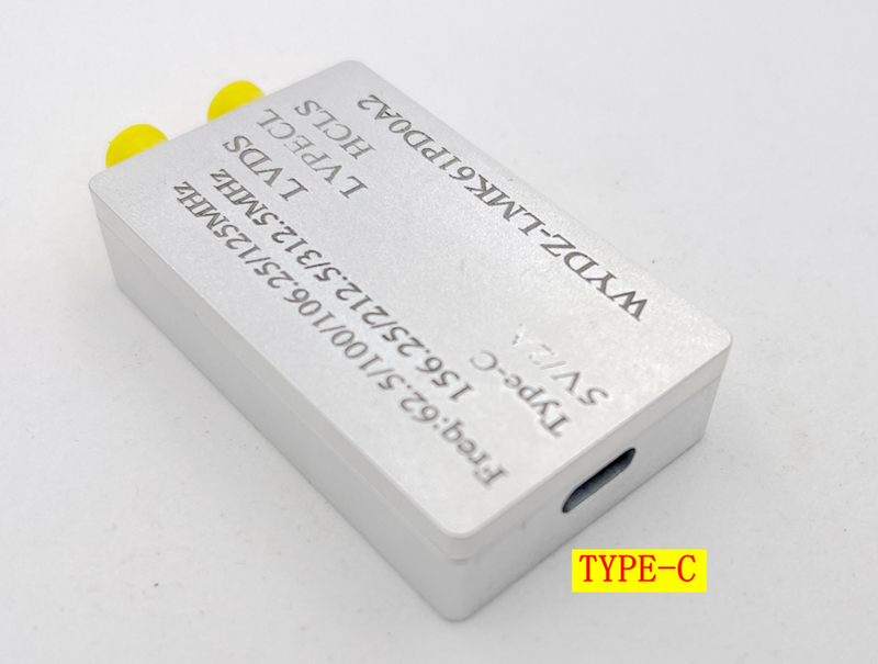
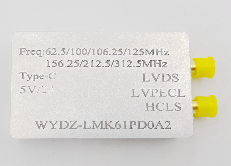
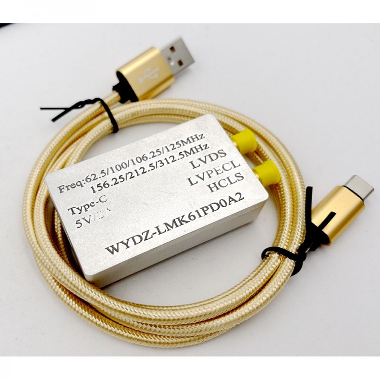
WYDZ-LMK61PD0A2 Oscillator Module 100MHz PLL Low Noise Differential Reference Source Multi-Frequency
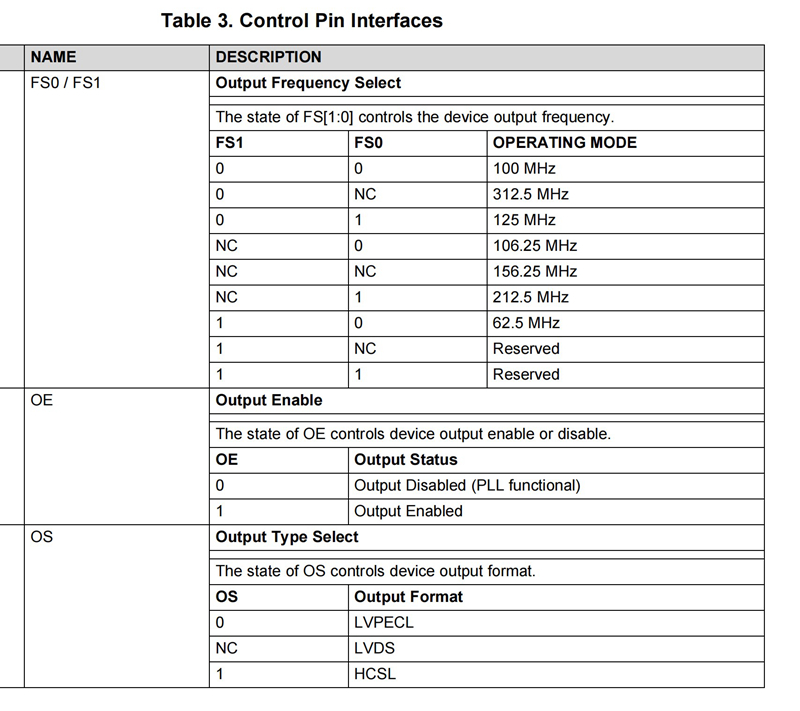
Parameters:
- Output frequency: 62.5M/100M/106.25M/125M/156.25M/212.5M/312.5M
- Differential output mode: LVPECL/LVDS/HCSL
- Power supply: TYPE-C (+5V)
- Control mode: internal jumper cap configuration output frequency and differential output mode
- The default jumper cap configuration when shipped is: 100MHZ, LVPECL output
- Module size: 60*36*14mm
- Output interface type: SMA (female)
Package Included:
- 1 x Oscillator Module (with fully shielded aluminum alloy shell)
- 1 x Type-C Cable
The Difference between Three Different Driving Methods:
The supported signal types are LVPECL (low voltage positive emitter coupling) logic), LVDS (low voltage differential signaling), HCSL (HighSpeed current guidance logic).
LVPECL stands for Low Voltage Positive Emitter-Couple Logic, which is low voltage positive emitter coupled logic, uses 3.3V or 2.5V power supply. To understand the LVPECL circuit, we must first understand the PECL circuit. PECL stands for Positive Emitter-Couple Logic, which means positive emitter coupled logic, and uses a 5.0V power supply. PECL evolved from ECL. ECL stands for Emitter-Couple Logic, which is also known as Emitter-Couple Logic. This circuit is a non-saturated digital logic circuit. The transistors in the circuit work in the linear or cut-off region, and the speed is not limited by the storage time of minority carriers, so it is the fastest in all kinds of existing logic circuits. One of them, can meet the working rate of up to 10Gbps. ECL has two supply voltages VCC and VEE. When VEE is grounded and VCC is connected to a positive voltage, the logic at this time is called PECL; when VCC is grounded and VEE is connected to a negative voltage, the logic at this time becomes NECL, and VEE is generally connected to a -5.2V power supply; ECL in the general narrow sense is Refers to NECL. Because PECL/LVPECL can share a positive power supply with other circuits in the system, PECL/LVPECL is more widely used than ECL. At first, PECL devices connected VCC to +5V. Later, in order to directly use the widely used 3.3V and 2.5V voltages, LVPECL (Low Voltage PECL) with VCC=3.3V/2.5V appeared.
LVDS (Low Voltage Differential Signaling) is a low-swing differential signal technology, which enables signals to be transmitted on differential PCB line pairs or balanced cables at a rate of several hundred Mbps. Its low-voltage amplitude and low-current drive output are realized In order to achieve low noise and low power consumption. LVDS (Low Voltage Differential Signaling) is a small amplitude differential signal technology. LVDS signal transmission generally consists of three parts: differential signal transmitter, differential signal interconnector, and differential signal receiver.
Each HCSL output pin of HCSL switches between 0 and 14mA. When one output pin is low (0), the other is high (driving 14mA). The equivalent load resistance of the HCSL driver is 68Ω, which is connected in parallel with a 50Ω resistor, which is equivalent to 28.81Ω. The swing of CML input is 14mAx28.81Ω=403mV. A 10nF AC coupling capacitor should be placed in front of the CML receiver to block the DC level from the HCSL driver. In addition, the internal self-bias of the CML receiver input must be confirmed. If there is no self-bias for the CML input, a 50Ω termination resistor to VCC must be placed on the PCB where the CML bias and the transmission line are terminated.
Control Method & Internal Diagram: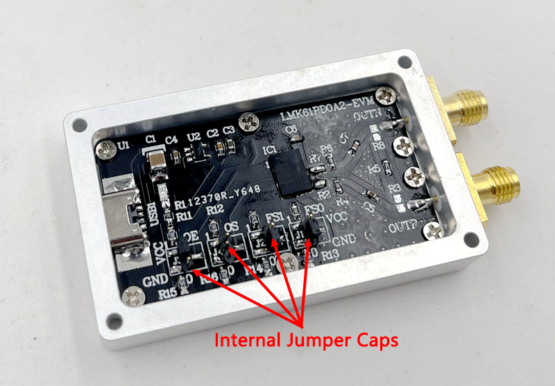
Reserved Hardware Interface: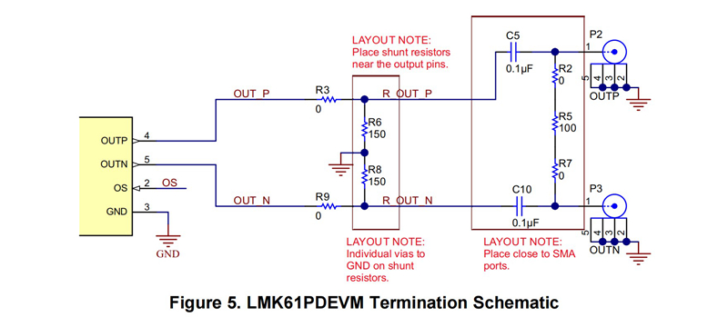
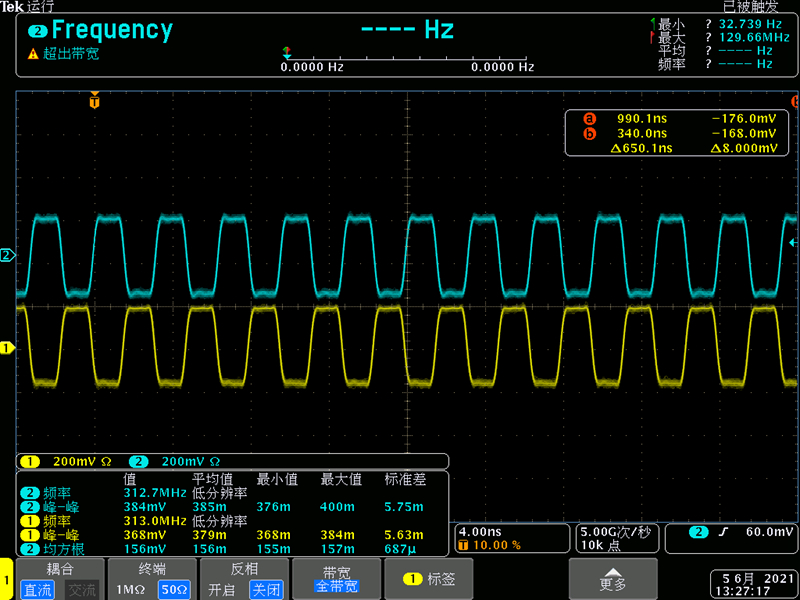
Measured Waveform:
1. 62.5M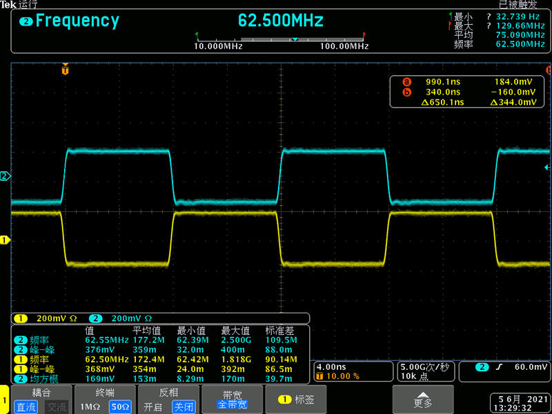
2. 100M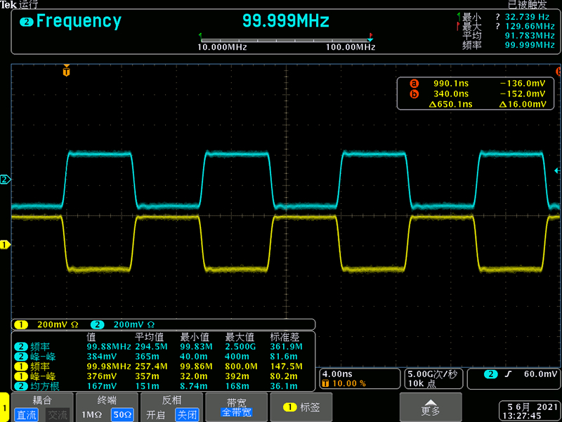
3. 106.25M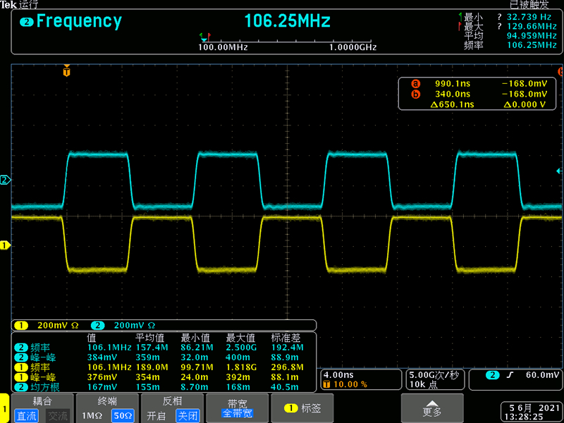
4. 125M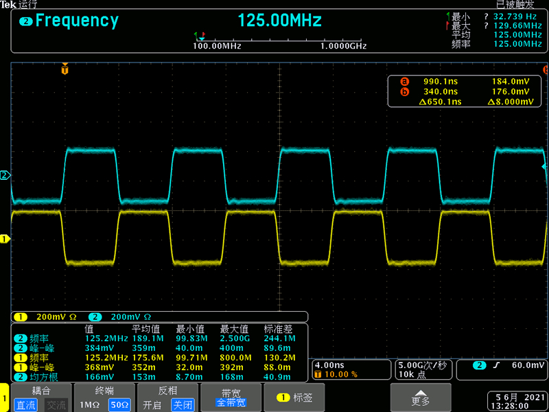
5. 156.25M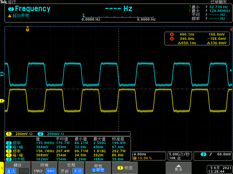
6. 212.5M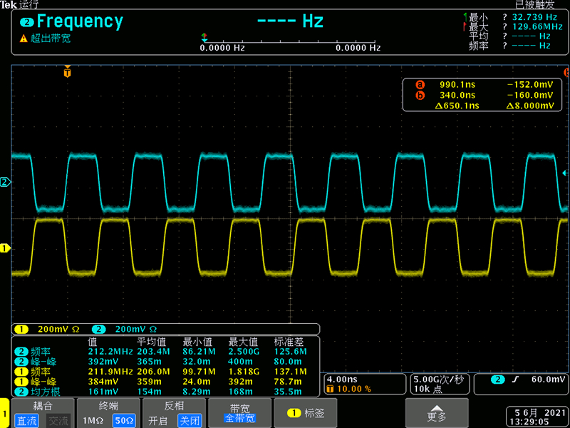
7. 312.5M