| Quantity | 3+ units | 10+ units | 30+ units | 50+ units | More |
|---|---|---|---|---|---|
| Price /Unit | $47.88 | $46.91 | $45.44 | $43.49 | Contact US |
 AXera PI Zero Module 5MP AI-ISP Camera Module Designed with SoC Chip AX620Q+SC450AI Image Sensor
$67.98
AXera PI Zero Module 5MP AI-ISP Camera Module Designed with SoC Chip AX620Q+SC450AI Image Sensor
$67.98
 0.5-inch 1024X768 OLED Driver Board High Quality Circuit Board for V760A-5 Wearable Head Mounted Display
$40.24
0.5-inch 1024X768 OLED Driver Board High Quality Circuit Board for V760A-5 Wearable Head Mounted Display
$40.24
 1PCS SFP+ Dual Mode Optical Module Small Form-factor Pluggable Transceiver Support 10Gbps Transmission with LC Interface
$26.09
1PCS SFP+ Dual Mode Optical Module Small Form-factor Pluggable Transceiver Support 10Gbps Transmission with LC Interface
$26.09
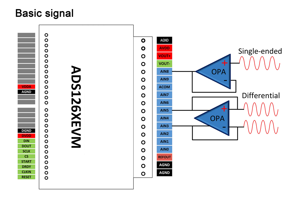
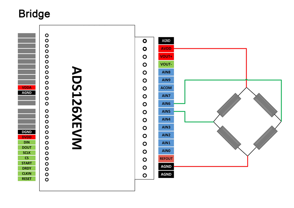
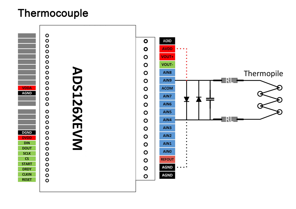
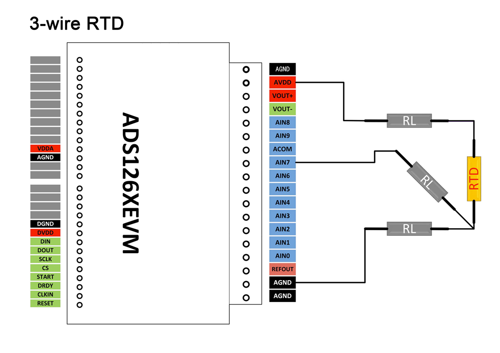
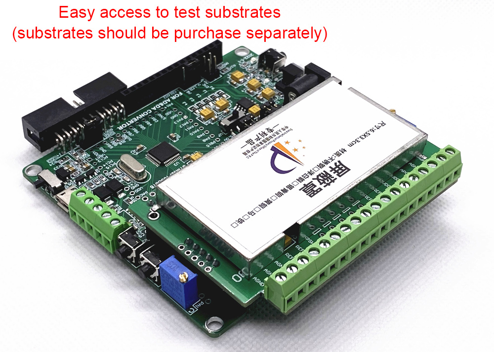
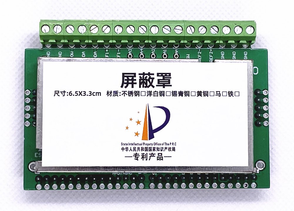
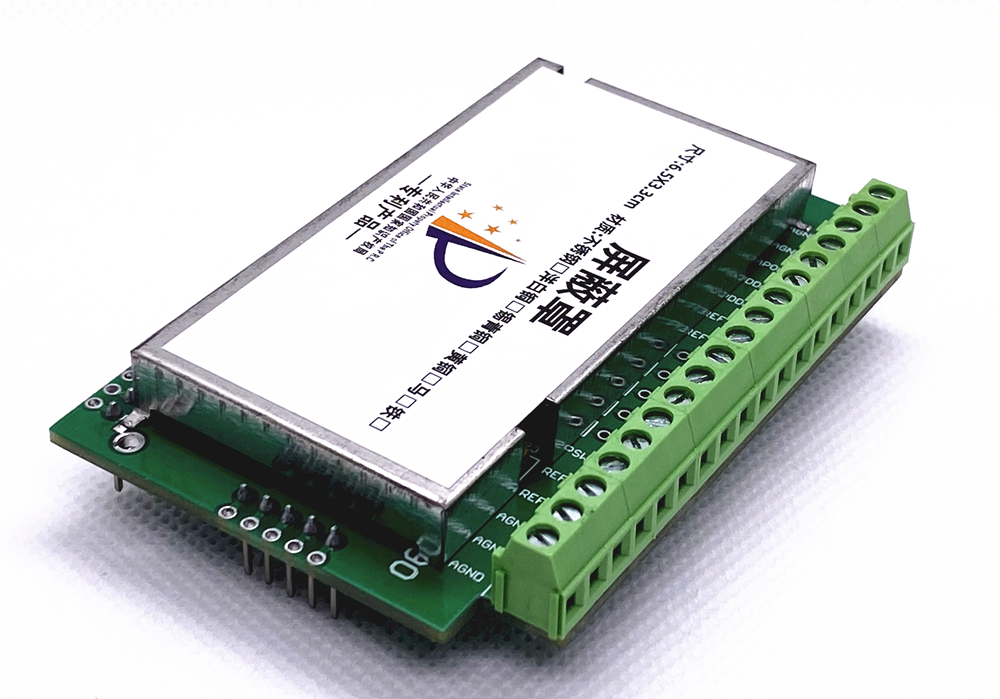
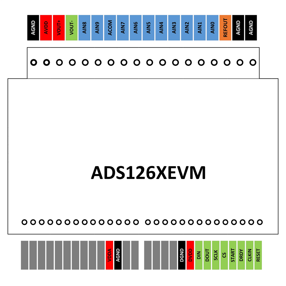
ADS1262 Industrial Version 32Bit ADC Module Analog to Digital Converter Module with Shielding Case
Features:
* Resolution: 32-bit
* Number of channels: 5 differential/11 single-ended
* Maximum sample rate: 38ksps
* Differential input voltage: ±VREF/Gain
* Programmable gain: 1-32
Package Included:
* 1 x ADC module
Functional framework diagram: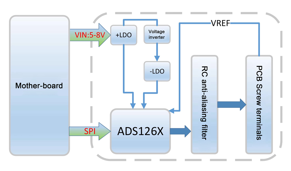
Version Comparison:
The difference between ADS1262 and ADS1263: ADS1263 integrates a 24-bit auxiliary delta-sigma ADC dedicated to background measurements. There is no difference in accuracy!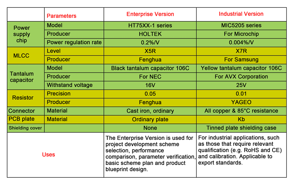
Advantages:
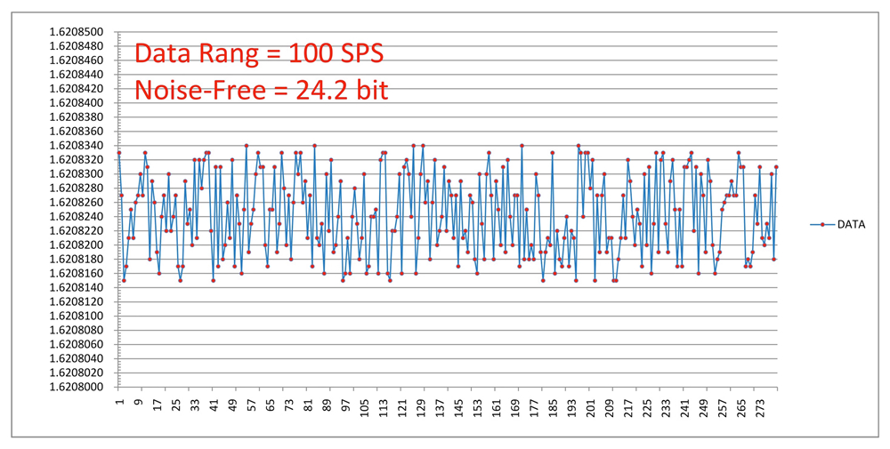
* 32bit ADC: At Data Rate = 20 SPS, the noise is only 0.16uVP-P, which is excellent compared to those of a 24-bit ADC. The chip manufacturer directly positions it in high-end industrial applications where higher temperature control is required, such as oil exploration. This satisfies the requirements of the PLC in the full temperature range, and the dual excitation current sources improve the matching of the RTD and provide excellent temperature compensation during bridge testing.
* To effectively reduce voltage noise, a clean LDO power supply with high PSRR and low ripple must be used. An anti-aliasing filter that uses a metal film resistor and MLCC as signal inputs is adopted. This reduces electrical noise from resistors and capacitors. When designing a PCB, the balanced layout of the thermal components and the placement of the decoupling capacitors are very important, especially the correct decoupling of the REF pin (the 8th pin of the chip) to achieve optimal performance.
* Reference design: Strictly follow the reference design requirements of the manual.
* Reference chip: A low-drift precision reference chip is used, and the reference output pin uses a capacitor with a large ESR to store enough charge to ensure the stability of the reference voltage when the ADC's internal conversion capacitor is extracted. If there is no buffer inside the chip, users will also need to add a low-noise follower as a buffer.
* Single-point grounding: The complete separation of analog ground and digital ground and the last single point of access to the power ground prevent the ground signals from being cross-linked with each other and bringing noise into the signal link.
* High-quality linear power supply: Noise from the power supply can reduce the effective resolution of the data converter if it contaminates signal input sources. A LDO chip with a high power supply rejection ratio and low ripple produces a clean and stable voltage rail to power the analog components. This is helpful for precision signaling systems.
* Pre-filter: low-temperature drifting metal film resistor + C0G multilayer ceramic capacitor constitute a low-pass filter. This improves total harmonic distortion, reduces resistive and capacitive electronic thermal noise, and provides the ADC with an excellent anti-aliasing filter that avoids aliasing noise contaminating the signal. At the same time, it eliminates the effects of overdrive signals outside of the filter bandwidth.
* PCB heat dissipation: The high-density use of vias in the copper area of the PCB forms an array to improve longitudinal Z heat dissipation and allow the components on the heating surface to cool down quickly. This can effectively avoid the concentration of hot spots on the PCB, and reduce the on-chip reference drift caused by the temperature rise.
Performance Tests: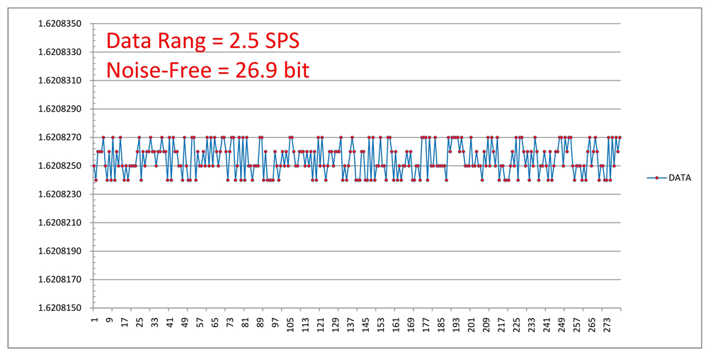

Application: